One of the first things I was told when I first started designed power electronics was to rate your semiconductors breakdown voltage 1.2 - 1.5x higher than your DC bus voltage. Examples -
If you have a 800V DC bus, your semiconductors should be rated for 1200V
If you have a 450V DC bus, your semiconductors should be rated for 600V
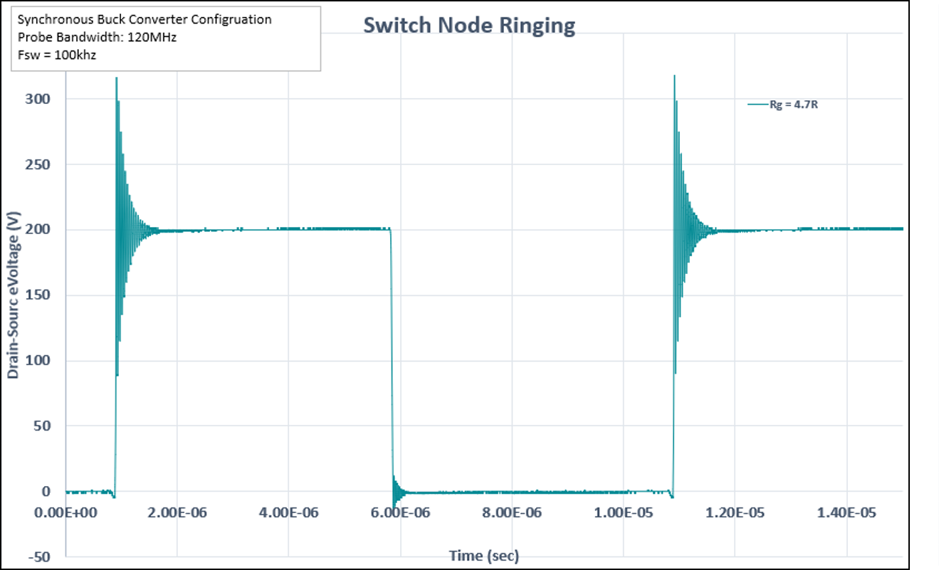
Figure 1: Measured ringing on switch node of synch. buck converter
Where does this rule of thumb come from? If you measure the switch node voltage with a high bandwidth probe, you’ll see that there is large voltage overshoot and subsequent oscillations (ringing). This is shown in Figure 1.
In this article, I’m going to attempt to distill this phenomenon down to its first principles and explain what’s going on in simple terms. I will then present several different ways to reduce overshoot and the duration of the ringing.
Note: Although I refer to MOSFETs in the article, the analysis also applies to IGBTs.
The Problem with Voltage Overshoot and Ringing
There are two major concerns -
Voltage Overshoot: Exceeding the breakdown voltage of the MOSFET
Ringing: Conducted and Radiated Noise (EMI)
First, you need to ensure that the voltage overshoot does not exceed the maximum blocking voltage of the device. Specifically,
Equation 1
where V_bus = DC bus voltage, ΔV_0-peak = maximum bus voltage ripple, ΔV_overshoot = voltage overshoot, SM = safety margin, and V_DS = Drain-Source voltage of MOSFET
Second, high dv/dt from ringing can lead to induced currents through capacitive coupling and can also act as an antenna to radiate EMI.
Where Voltage Overshoot Comes From
For this analysis, we are going to look at a synchronous buck converter. Note this is pretty much the same thing as one leg of a three-phase inverter connected to a RL load so this analysis can be applied to that as well.
Figure 2: Synchronous Buck Converter Schematic. Parasistics not shown
The high frequency power commutation loop is the path formed between the DC link capacitor and the power semiconductors. This loop does all the heavy lifting… that is, there are high currents and high voltages switching at very high frequencies.
In electrical engineering, two things are needed for resonance to occur, an L and a C. Every conductor has parasitic resistance and stray inductance and every semiconductor exhibits some sort of output capacitance when its switched off. The values are very small (pF and nH), but when you’re switching 10kV/μs, that’s enough to excite these parasitic resonant circuits and cause oscillatory behavior.
The voltage overshoot manifests itself at the time when one MOSFET is turned on, while the other MOSFET is carrying freewheeling current. This happens when you’re in the deadtime period of the switching cycle. It’s important to understand this so let’s go through the switching cycle state-by-state. We are going to assume the buck converter is operating at an arbitrary duty ratio with an inserted deadtime to prevent shoot-through. Note: the parasitic DC Link inductance is shown in the schematics below.
State 1
For the start of the switching cycle, we are going to assume the low-side switch is closed - so, current is flowing through the load and the low-side switch as shown by the red path.
Figure 3: State 1 - Low-side switch is closed
State 2
The low-side switch opens and the deadtime period begins. Because the output inductor is stiff, current must continue to flow. The current takes a path through the MOSFET’s intrinsic body diode.
Figure 4: State 2 - Low side switch opens and deadtime period begins
State 3
Once the deadtime period ends, the high-side switch closes. At this moment, there is an effective short circuit due to the reverse recovery charge of the body diode. Because the circulating current is stiff, it can’t instantaneously stop so the net forward current is equal to the DC link current minus the circulating load current. Regardless, this is large excitation in the current.
Figure 5: State 3 - Deadtime period ends, High-side switch closes
State 4
Once the reverse recovery period of the diode ends, the low side switch presents a capacitive load to the circuit and an RLC circuit is formed. The R is the on-state resistance of the high side switch. The L is the summation of stray inductances in the commutation loop. The C is the output capacitance of the low side switch.
Figure 6: State 4 - Reverse recovery period of diode ends, Low-side switch presents cap load to circuit
eQUIVALENT cIRCUIT FOR oVERSHOOT aNALYSIS
From this we can form an equivalent circuit that we can use to analyze the behavior of the RLC circuit.
R_DS,ON is the on-state resistance of the high-side switch. This is the damping element in the second order system. We typically want to minimize this to reduce conduction losses and maximize efficiency. This causes the circuit to be underdamped and voltage overshoot will occur across C_OSS which is, in effect, across the low-side switch.
Figure 7: Equivalent circuit for overshoot analysis
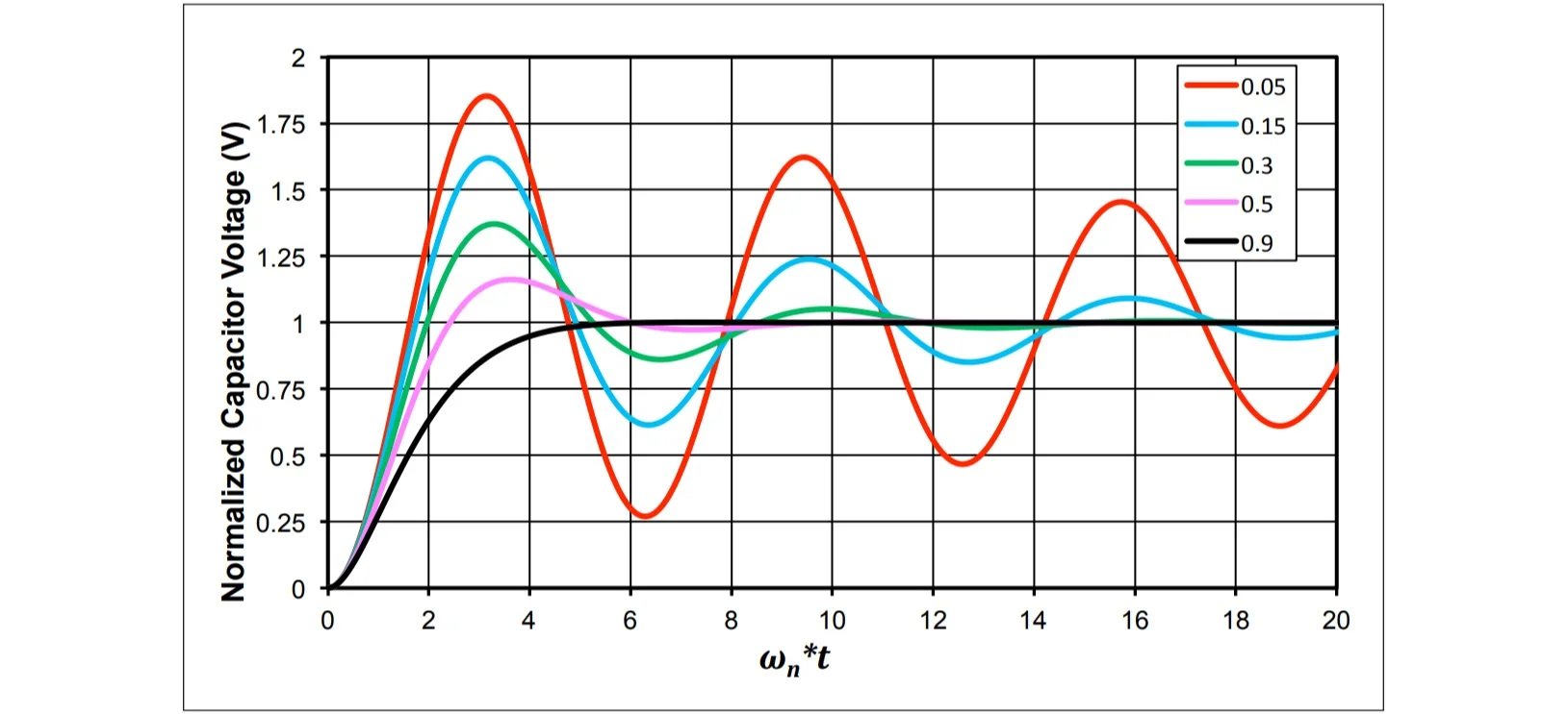
The RLC series circuit is a classic second order system with characteristics that are shown in Figure 8. The normalized capacitor (C_OSS) voltage is plotted against time. Each trace represents different damping ratios.
Figure 8: Normalized capacitor voltage (C_OSS) vs. ω_n * t for various values of ζ (damping ratio)
We can see that as damping ratio approaches unity, the overshoot and settling time is reduced. The damping ratio can be solved for using equation 2.
Equation 2
As mentioned above, we want R to be as small as possible in order to reduce conduction losses. C is fixed since this is the output capacitance of the switch. So the only thing we can do is minimize DC Link inductance.
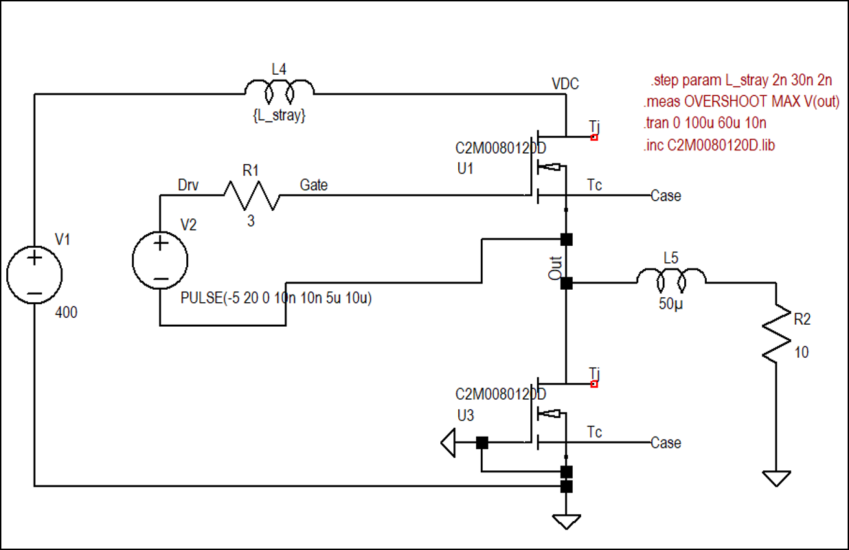
An LTSpice circuit simulation was run to prove this fact. You can see the near linear increase in voltage overshoot as DC link inductance is stepped from 2nH to 30nH.
Figure 9: LTSpice simulation schematic for evaluating how changes in DC link inductance affect ringing on the switch node.
Figure 10: Plot showing relationship between voltage overshoot vs DC link stray inductance
How to reduce voltage overshoot and ringing
Here are a few ways you can reduce voltage overshooting and ringing. There are probably other ways so if you know one that’s not listed here, leave a comment!
1. Minimize DC link inductance - Loop area needs to be minimized! High frequency film capacitors with low ESL should be used. These should be placed as close to the power terminals as possible. The DC link connections should be planar laminated busbars or a PCB with power layers that are adjacent. If you really need to optimize the DC link, a multiphysics tool such as COMSOL should be used to analyze high frequency current paths to maximize magnetic field cancellation. WolfSpeed did an excellent study on this [2] and their optimized busbars for their inverter are shown below.
Figure 11: DC laminated bus structure under study for Wolfspeed’s 250 kW traction inverter. [2]
Figure 12: Wolfspeed’s 16 kg, 250 kW SiC based liquid-cooled, three - phase inverter. [2]
Figure 13: Gate Resistance vs. Voltage Overshoot. Same schematic that’s shown in Figure 9 was used for this analysis - 400V DC bus, synchronous buck converter, RL load, etc.
2. Increase gate resistance - Slowing down the switching speed is another way to reduce overshoot. This will increase switching loss, but if you’re not meeting your EMC requirements and you don’t have time to do another layout iteration, this is an option. The effect of changing the gate resistor on the voltage overshoot can be seen in the plot below. As the gate resistance is stepped from 1 to 20 ohms, the overshoot decreases almost linearly.
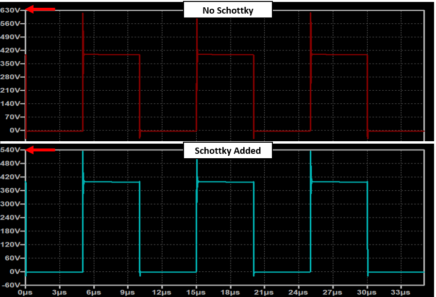
3. Add a Schottky diode in parallel with the MOSFET body diode - Schottky diodes have near zero reverse recovery current. This will reduce the current step excitation to the parasitic RLC circuit. Note: I have never done this in practice, but simulation shows a reduction in voltage overshoot by almost 90V with an external schottky diode added.
Figure 14: A comparison of ringing on the drain-source voltage waveforms with and without an external schottky diode. There is almost a 90V reduction.
Figure 15: RC snubber is added in parallel with the low-side switch to reduce ringing.
4. Add a RC Snubber Network across the low-side MOSFET - A properly designed snubber can virtually eliminate parasitic ringing. A method for designing the snubber is outlined in [3]. Like all things in engineering, there is no such thing as a free lunch. Power is lost in the snubber circuit every switching cycle. This is known as snubber loss.
P = 1/2 * C * V^2 * Fsw
* Note: I have never done this in practice before either. Recommendation is based on literature I’ve read.
Important Things to Note
Figure 16: Graph of MOSFET capacitance from CAB450M12XM3 datasheet
MOSFET Output Capacitance Changes with Bus Voltage
The MOSFET capacitance changes as a function of bus voltage. It sharply decreases initially and then tapers off. The implications of this is that at lower bus voltages, the percent overshoot will be higher. Conversely, at higher bus voltages, the percent overshoot will be lower.
Figure 17: Feedback/Miller capacitor that connects from gate to drain of MOSFET. Induced currents can lead to parasitic turn-on.
Coupling to Gate
Large dv/dt from ringing can induce currents in the gate drive through the feedback capacitance (C_GD). This is also called the Miller capacitance. This can raise the gate-source voltage and, in some cases, parasitically turn-on the MOSFET, which can lead to shoot-through.
Some gate drivers feature a “Miller clamp” which provides a low-impedance path for parasitic charge to flow. This strong pulldown on the gate is useful for preventing parasitic turn-on. If you are driving the MOSFET off with a negative voltage, you typically don’t have to worry about this too much.
Implications for Silicon Carbide and GaN
In general, standard guidelines developed for IGBTs also apply to SiC and GaN switches. However the significantly faster switching speed of these devices require you to be much more careful with your layout and high frequency power loop design. Dv/dt and di/dt are much higher with these devices so parasitic inductance and capacitance must be reduced as much as possible.
Figure 18: SiC half-bridge [4]
Conclusion
Hopefully this article gave you some insight on why ringing/overshoot and some things you can do to reduce it. With the rise of SiC and GaN and their fast switching speeds, these considerations are especially important.
Completely mitigating ringing and overshoot in “conventional” hard-switched inverter applications requiring substantial power throughput is infeasible. If you want to achieve critical damping, the on-state resistance of your MOSFET would have to be significant. See the damping ratio equation 2. This is undesirable as it increases your conduction losses. Just recognize that you will always have ringing/overshoot and that there is a tradeoff between switching speed and EMC. There will be an optimum gate resistor value that balances voltage overshoot/EMC and switching speed. But, just keep in mind that one of the main advantages of SiC and GaN is the fast switching speed and if you use too high of a gate resistor, you nullify this. The best thing you can do preserve this advantage is optimize the layout of the high frequency power loop to minimize inductance as much as possible. This is crucial if you’re trying to optimize for efficiency and power density, but still need to maintain a reasonable level of EMI.
References
[2] https://ieeexplore.ieee.org/abstract/document/8095886


![Figure 11: DC laminated bus structure under study for Wolfspeed’s 250 kW traction inverter. [2]](https://images.squarespace-cdn.com/content/v1/5b9b0eb14611a095d6589969/1570157384993-S2IVG1SOJBBI5A5SU1QC/busbars.jpg)
![Figure 12: Wolfspeed’s 16 kg, 250 kW SiC based liquid-cooled, three - phase inverter. [2]](https://images.squarespace-cdn.com/content/v1/5b9b0eb14611a095d6589969/1570157349762-1BUVCC0W48ZMT8TH5LE4/image-asset.png)


![Figure 18: SiC half-bridge [4]](https://images.squarespace-cdn.com/content/v1/5b9b0eb14611a095d6589969/1570217731130-OAZD5E72NQAROK464SYB/SiCGateDriver+-+top.PNG)